Silicon, a versatile and abundant element, has been the cornerstone of modern technology for decades. The widespread adoption of silicon-based technologies has revolutionized communication, computing, and energy production, profoundly shaping the contemporary world.
Overview of Silicon
Properties and Characteristics of Silicon
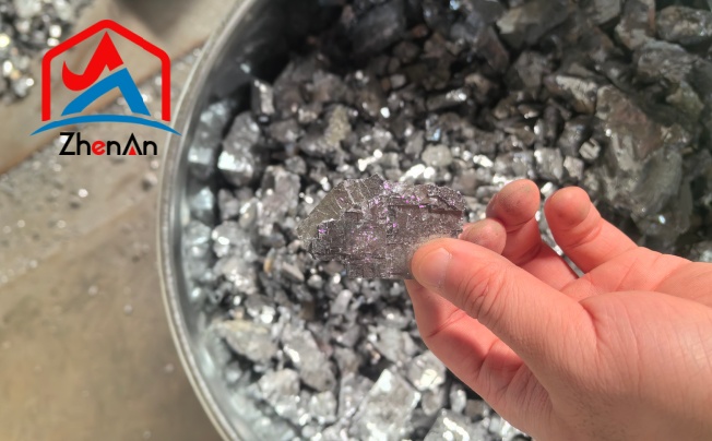
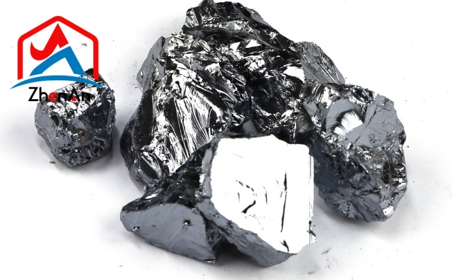
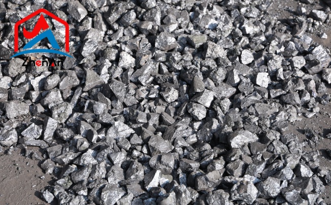
Silicon, a chemical element with the symbol Si and atomic number 14, is widely known for its semiconductor properties. It possesses a crystalline structure and is a hard, brittle material with a metallic luster.
Silicon exhibits interesting electrical properties due to its unique position in the periodic table, allowing it to conduct electricity under certain conditions. Moreover, silicon has a high melting point of 1414 degrees Celsius and is abundant in the Earth's crust, making it an economically feasible material for various applications.
Dominance of Silicon in Electronic Devices and Solar Panels
The dominance of silicon in electronic devices and solar panels stems from its excellent semiconducting capabilities. In the realm of electronics, silicon serves as the foundation for integrated circuits, microprocessors, and various components used in computers, smartphones, and other digital devices. Its ability to control the flow of electrical current efficiently has made silicon indispensable in modern technology.
Furthermore, silicon plays a crucial role in photovoltaic cells used for solar energy generation. Its abundance and well-established manufacturing processes have propelled silicon-based solar panels to prominence as a sustainable energy solution.
Limitations and Challenges Associated with Silicon
Despite its widespread use and effectiveness as a semiconductor material, silicon does have inherent limitations that drive the search for alternatives. One significant limitation is that traditional silicon-based electronics are reaching their physical limits in miniaturization due to quantum effects becoming more pronounced at smaller scales. This poses challenges for further advancements in computing power without alternative materials or technologies.
Additionally, the manufacturing process of crystalline silicon solar cells can be energy-intensive and costly, impacting their overall sustainability. Overcoming these challenges while improving efficiency remains crucial for the future development of electronic devices and renewable energy technologies.
Emerging Materials as Potential Replacements for Silicon
Graphene
Graphene, an extraordinary two-dimensional carbon lattice, is emerging as a promising candidate to replace silicon in various electronic applications. Its unique properties, such as high electron mobility and excellent thermal conductivity, make it highly desirable for next-generation electronics.
Graphene's potential applications range from ultra-fast transistors and flexible displays to transparent conductive films and energy storage devices. With its ultrathin structure, graphene has also shown promise in creating wearable technology that seamlessly integrates with our daily lives.
However, one of the major challenges hindering the large-scale production and integration of graphene into devices is the lack of a cost-effective manufacturing process. Current methods involve exfoliating graphite or synthesizing graphene through chemical vapor deposition on metal substrates.
These processes are time-consuming and expensive for commercial production. Researchers are actively exploring innovative techniques to overcome these limitations and achieve scalable graphene production methods that can be easily integrated into existing manufacturing processes.
Gallium Nitride (GaN)
Gallium Nitride (GaN) stands out as a material with superior properties when compared to silicon in power electronics and LED lighting applications. GaN has a higher breakdown voltage capability, enabling efficient power conversion with reduced energy losses.
This characteristic makes it ideal for high-power applications like electric vehicle chargers or data center power supplies where energy efficiency is crucial. Despite its advantages over silicon, GaN faces certain limitations that need further research and development to be addressed effectively.
One challenge lies in achieving consistent material quality across larger wafer sizes required for commercial production, which impacts device performance and reliability. Researchers are actively working on refining manufacturing techniques like epitaxial growth to enhance material quality while reducing costs associated with equipment upgrades.
Carbon Nanotubes (CNTs)
Carbon Nanotubes (CNTs) have garnered significant attention due to their exceptional electrical conductivity and remarkable mechanical strength properties. CNTs possess an impressive aspect ratio with diameters of just nanometers while being thousands of times longer—an ideal combination for creating miniature yet robust electronic components.
The progress made in CNT-based transistors holds great promise for future electronics where conventional silicon-based transistors reach their physical limits due to heat dissipation issues at nanoscale dimensions. Additionally, CNTs show potential in revolutionizing battery technology through their ability to store large amounts of charge per unit mass compared to traditional lithium-ion batteries.
Moreover, sensors based on CNTs offer ultra-high sensitivity and selectivity suitable for various fields such as healthcare diagnostics or environmental monitoring systems. Continued research efforts focus on optimizing CNT synthesis methods at scale while ensuring control over chirality—the arrangement of atoms along the nanotube axis—to harness their full potential in advanced electronic devices.
Other Promising Materials on the Horizon
- Quantum Dots
Quantum dots are tiny semiconductor particles that exhibit extraordinary optical properties due to their quantum confinement effect. These nanocrystals, typically measuring only a few nanometers in diameter, possess tunable emission spectra and exceptional color purity.
These characteristics make them highly attractive for applications in displays and lighting. Quantum dot-based displays have the potential to deliver a wider color gamut, enhanced brightness levels, and improved energy efficiency compared to traditional liquid crystal displays (LCDs) or organic light-emitting diode (OLED) screens.
Furthermore, quantum dots can be precisely engineered to emit specific colors by varying their size or composition. This capability opens up possibilities for vibrant and accurate color reproduction in visual technologies.
Additionally, quantum dots can be integrated into LEDs to create highly efficient lighting solutions with better color rendering and lower power consumption. Although challenges remain in scaling up production and addressing concerns related to toxicity, ongoing research is focused on finding novel approaches for large-scale synthesis of quantum dots using environmentally friendly materials.
- Topological Insulators
Topological insulators are a class of materials that have gained significant attention due to their unique electronic properties. Unlike conventional insulators that prevent the flow of electrons through their bulk structure, topological insulators allow electron transport along their surfaces while remaining insulating internally.
This intriguing behavior makes them promising candidates for applications in next-generation electronics and ultra-fast computing. The surface states of topological insulators exhibit exotic phenomena such as spin-momentum locking and robust protection against scattering processes.
These properties could revolutionize information processing by enabling faster data transfer rates and more efficient energy utilization compared to current technologies. Moreover, the potential use of topological insulators in quantum computing holds tremendous promise due to their ability to host protected qubits that are less susceptible to decoherence.
Researchers are actively exploring various methods for synthesizing topological insulator materials at different scales and investigating ways to manipulate their unique surface states effectively.


